Hamamatsu Photonics | Optimize printed electronics manufacturing with laser sintering

Breaking News:
Kathmandu Nepal
Donnerstag, März 19, 2026

While already common in various industries, production equipment for printed electronics still has room for improvement to optimize manufacturing efficiency. One important aspect of this optimization, especially when using metal nanoparticle inks, is the sintering process. The sintering step includes fusing the metal nanoparticles in ink ensuring the required low resistivity of the finished circuits. For this task, heating ovens, NIR emitters, and broadband flash lamps are established technologies, but they suffer from drawbacks that limit the speed or efficiency of production.
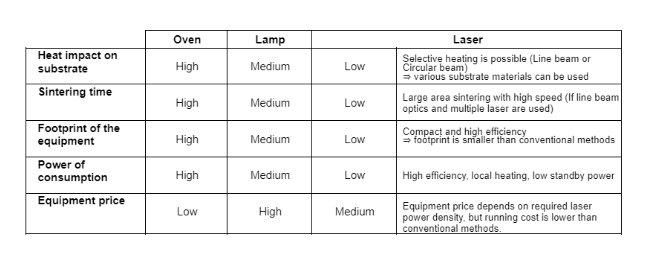
In this article, we present five aspects of printing equipment that can be improved by switching to laser sintering.
We are exhibiting!
Visit our booth at The Future of Electronics RESHAPED Europe – the flagship TechBlick event. This event will take place at the Estrel Hotel and Convention Center (ECC) in Berlin on 23-24 October 2024. Explore the preliminary agenda here.
1. Reducing the footprint of the printing machine
Furnaces for sintering printed electronics can be large, particularly for serial production. As the sintering process in the oven takes a few to tens of minutes, it typically does not match the production rate of the preceding printing process. To maintain high production rates, more furnaces or long conveyors are required, resulting in a large machine footprint.
Laser sintering offers a solution for developing more compact machines. Since the sintering process using NIR laser takes only milliseconds, it can be performed on the conveyor directly after printing, making roll-to-roll processes possible. For machines with limited space, laser sintering provides even more flexibility. As the laser light is coupled into a fibre, it can be flexibly guided over longer distances, allowing separation of the light output from the laser source and its electronics. This minimizes the space required at the light output, enabling smaller sintering machines for confined production areas.
2. Increase production speed
Switching from a furnace-based sintering process to laser sintering reduces space requirements and helps increase production speed. While the sintering process in a hot air oven takes a few to tens of minutes, NIR laser light sinters the metal ink within milliseconds. This allows high printing speeds and ensures that the sintering step is no longer the production bottleneck. Laser sintering significantly enhances production speed due to the easily scalable laser power, which maintains precise focus with line optics. Depending on the ink and substrate, laser technology allows for speeds of several hundred millimeters per second in roll-to-roll production, substantially increasing output rates.
3. Optimizing energy efficiency
Energy efficiency is now one of the most important aspects of any production process. Minimizing energy consumption is essential to meet sustainability goals and to reduce production costs, given rising energy prices.
The production of printed electronics involves many energy-intensive processes. One example is the sintering step, which requires intense heating to achieve the desired conductivity of the ink, often exceeding 100°C, depending on the nanoparticles. It is an energy-intensive process with significant production costs. Large ovens, commonly used for this process, must heat both the part and the air inside the oven to the target temperature, consuming substantial amounts of power, often 60kW or more. Alternative sintering technologies, such as photonic sintering, also demand considerable power. For instance, flash lamps used during a roll-to-roll process require 5kW of electrical power or more.
Laser sintering offers a more energy-efficient solution, due to its high conversion efficiency from electrical power to light power and excellent conversion rate. Typical laser sources for laser sintering, such as the Hamamatsu SPOLD® [1,2] consume around 1kW, while still enabling fast roll-to-roll production. This improved efficiency can significantly reduce production costs over the lifetime of a production machine.
We are speaking!
Listen to our presentation at The Future of Electronics RESHAPED Europe – the flagship TechBlick event. This event will take place at the Estrel Hotel and Convention Center (ECC) in Berlin on 23-24 October 2024. Explore the preliminary agenda here.
4. Enabling the use of thermo-sensitive materials
One of the significant advantages of printed electronics is the versatility of substrates, enabling electronics to be integrated into various materials like packaging or clothing. However, high sintering temperatures, typically around 200°C for materials like silver nanoparticles, limit the substrates that can be used. For instance, plastics such as polyethylene (PE) begin to soften at temperatures above 70°C, making it impractical to sinter them in furnaces operating at 200°C or higher.
Laser sintering provides the solution. As ink and substrates have different absorption properties, it is possible to select a wavelength where the light is only absorbed in the ink while the substrate remains transparent. As a result, only the ink is heated to the required sintering temperature while the substrate remains unaffected. This allows thermo-sensitive materials, such as plastic foils, to be used, which is advantageous for the packaging industry.
However, heat dissipation from the ink into the substrate can still indirectly heat and damage it. Therefore, it is essential to tailor the heating illumination to the properties of the materials. Laser sintering has many advantages over photonic sintering using flash lamps as the optimum wavelengths can be chosen depending on the application. The Hamamatsu SPOLD®, for example, is available at 940nm (optional 808nm), minimizing substrate heating compared to the broader spectrum of tungsten lamps.
The laser also offers more precise control of power compared to flash lamps, allowing fine adjustment to stay below the melting temperature of the substrate. This precise control further reduces potential substrate damage, crucial when printing on highly thermo-sensitive materials like PET.
5. Reducing ink costs
In addition to the flexibility of substrates, one of the significant advantages of printed electronics is the low production cost. Laser sintering can further reduce costs by switching to less expensive inks. Due to the silver nanoparticles dissolved in the ink, it becomes quite an expensive consumable. Indeed, cheaper alternatives, like copper or aluminium offer similar conductivity values but require different sintering parameters to find the optimum conductivity, strength, and adhesion results.
For this optimization, the flexibility of laser sintering is beneficial. Hamamatsu collaborates with several ink manufacturers worldwide to support manufacturers when switching ink materials. Together, they test several micro and nano ink formulations to find their optimum sintering parameters, giving customers a head start when switching to cheaper inks.
Laser Sintering increases productivity
Switching to laser sintering can significantly impact the productivity of printed electronics production. The laser adds the necessary flexibility to your process and enables the optimization of important parameters like resistivity, density, and adhesion by choosing the optimum ink type, laser power, or conveyor belt speed. Application tests are essential to maximize this increase in productivity. Hamamatsu Photonics supports customers with dedicated application engineers who conduct sintering tests to identify the optimum set of parameters. This simplifies the transition to new laser sintering technology and ensures customers get the most out of their printed electronics production.
For more information on our SPOLD® device or on this topic, please contact: info@hamamatsu.de
Author: Mr Naveen Balla, info@hamamatsu.de
References
[1] Hamamatsu Photonics, LD irradiation light sources (SPOLD®): www.hamamatsu.com/eu/en/product/lasers/applied-products-of-semiconductor-lasers
[2] Hamamatsu Photonics, "Weld, Solder, Cure or Sinter with SPOLD®": www.youtube.com/watch?v=I0sLZBR9u_I
[3] A Review on Printed Electronics, 2021: Fabrication Methods, Inks, Substrates, Applications and Environmental Impacts: doi.org/10.3390/jmmp5030089
Hamamatsu Photonics Deutschland GmbH
Arzberger Str. 10
82211 Herrsching am Ammersee
Telefon: +49 (8152) 375-0
Telefax: +49 (8152) 375-199
http://www.hamamatsu.com
![]()