Thin Chips and Robust Substrates – Key Technologies for Cost- Efficient Silicon Carbide Power Electronics
Semiconductor Technology on the Threshold of the Post-Silicon Era
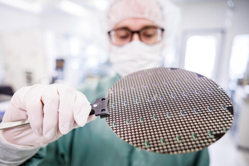
Power electronics based on the wide-bandgap semiconductor silicon carbide (SiC) are a key enabler for energy-efficient, sustainable and high-performance applications in electromobility – from cars and commercial vehicles to trains, ships and airplanes, in the generation, transportation and storage of renewable energies, as well as for IT and industrial infrastructures. It is therefore an important and competitively relevant factor for the current global transformation processes in the areas of mobility, energy and digitalization. The market for SiC power devices is expected to grow at an annual rate of over 30 percent. Compared to conventional silicon technology, the use of SiC power electronics in a standard drive converter saves more energy than is required to manufac-ture the SiC power electronics themselves.
While the technological advantages of SiC are obvious due to its physical properties, the higher costs compared to the established silicon are still an obstacle to faster market penetration. Chip costs are more than three times higher than for silicon. The initially required SiC wafer is the biggest cost driver here. In the case of a SiC-based metal-oxide semiconductor field-effect transistor (MOSFET), this accounts for more than 40 percent of the man-ufacturing costs. In addition, due to the unfavorable mechanical material properties and large thickness of the monocrystalline SiC wafer, electronics processed from it only achieve approx. 30 percent of the thermome-chanical service life compared to silicon. This disadvantage leads to an approx. 25 percent larger chip area and, in the case of an inverter for example, to around 25 percent higher costs in the application.
Cost-Effective SiC Substrates Without Sawing and Grinding
In the three-year ThinSiCPower project (2024-2027), funded by the Fraunhofer PREPARE program, researchers are developing an alternative way to produce cost-effective SiC substrates and significantly thinner SiC chips using more resource-efficient processing technologies. Rather than first sawing the expensive, high-quality SiC wafers with the usual material loss and later back-grinding them in device processing, the SiC crystal is separated directly into thinner wafers using a special laser process without any major loss of material, which are then bonded onto an inexpensive carrier substrate based on polycrystalline SiC.
With ThinSiCPower Towards a Full SiC Process Line, Made in Germany
Fraunhofer ISE, ENAS and IWM with the Fraunhofer IISB as project coordinator are pooling their individual com-petencies in ThinSiCPower. A SiC coating technology developed by Fraunhofer IISB is being adapted for the manufacturing of the poly-SiC carrier substrates, which is more cost- and resource-efficient than the conven-tional manufacturing method using chemical vapor deposition. The low-loss separation of the thin SiC wafers is carried out using a laser for defined mechanical pre-damage (Fraunhofer ISE) and subsequent separation under well-defined mechanical conditions for controlled crack propagation (Fraunhofer IWM). The wafer bonding process for the poly-SiC substrate with the split SiC, including the necessary surface preparation before and after the bonding process, will be developed at Fraunhofer ENAS, while the subsequent device processing and qualification will take place at Fraunhofer IISB. The partners are also developing adapted electrical test methods at thin wafer level as well as physics-of-failure simulation models to maximize the market acceptance of this new class of low-cost SiC substrates. With this, a broad applicability in the relevant industries could be achieved.
The aim is to reduce SiC device costs by 25 percent by developing technology for the production of cost-effective thin SiC wafers and poly-SiC substrates. In addition, SiC design costs are to be reduced by further 25 percent by increasing the load cycle stability by 300 percent. The target markets are semiconductor and power module manufacturers as well as their process and equipment suppliers through to test equipment suppliers. With this project, the participating partner institutes are also combining their expertise to set up a complete, highly innovative and future-oriented SiC processing line within the Research Fab Microelectronics Germany (FMD). The consortium is receiving consultancy support directly from partners in industry.
The ThinSiCPower project not only accelerates the market penetration of silicon carbide through the targeted cost reduction and conceptual advantages, but also serves to secure an innovative, resilient and industry rele-vant SiC technology value chain in Germany and Europe.
The Fraunhofer Institute for Integrated Systems and Device Technology IISB is one of Europe’s leading research institutions for wide-bandgap semiconductors and power electronics, covering the complete value chain. The spectrum ranges from basic materials, semiconductor devices and process technologies, power electronic modules and components to complete power electronic and energy systems.
Main target applications of the IISB are semiconductor manufacturing, electromobility, aerospace as well as sustainable energy supply. With its solutions, the institute has been setting benchmarks in energy efficiency and performance, even for extreme operating conditions. The integration of intelligent data-based functionalities also continuously opens up new application scenarios.
Fraunhofer IISB supports its customers and partners worldwide in transferring scientific results into commercial products. Its activities are organized in two business areas: Semiconductor Technology and Power Electronic Systems. A total of around 300 employees works at the headquarters in Erlangen, Bavaria, and at the Fraunhofer Technology Center High Performance Materials THM in Freiberg, Saxony.
Fraunhofer-Institut für Integrierte Systeme und Bauelementetechnologie IISB
Schottkystraße 10
91058 Erlangen
Telefon: +49 (9131) 761-0
Telefax: +49 (9131) 761-390
http://www.iisb.fraunhofer.de
![]()